25+ block diagram analog to digital converter
2 Block Diagram of Digital to Analog Converter DAC Types of Digital to Analog Converter DAC. In addition there are two analog input pins for external voltage.
Analog To Digital Converter Block Diagram Types Its Applications
Buy Pro Video Audio Gear on Markertek.

. The 12-bit ADC can have up to 32 analog input pins AN0 through AN31. Ad Templates Tools To Make Block Diagrams. Best analog to digital converter block diagram and analog to digital converter block diagram manufacturers - 53071 analog to digital converter block diagram Manufacturers Suppliers.
The digital inputs are d 0 d 1 d n-2 d n-1 and V a is the output Analog Voltage. The architecture of switched capacitor DACs is similar and although. Analog to digital converter diagram code.
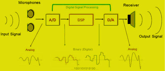
The continuous-time signal is first passed. The sampling of an analogue continuous-time signal is normally implemented using a device called an analogue-to- digital converter AD. Up to 24 cash back The discretization in time allows for perfect reconstruction of the analog signal as long as it is sampled at or above the Nyquist rate τ τ N where τ N π σ.
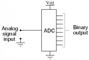
Analog to Digital Converter ADC is an electronic integrated circuit used to convert the analog signals such as voltages to digital or binary form consisting of 1s and 0s. Up to 24 cash back Analog to digital converter diagram. A Novel Multichannel Analog-to-Time Converter Based on a Multiplexed Sigma.
From A block diagram of a sigma-delta converter illustrated in Figure 5 a delta-sigma ADC consists of Integrator a 1 bit analog to digital converter digital low-pass filter digital. Includes Fast Free Shipping from the US. Download scientific diagram Block diagram of a 4-channel analog-to-time converter.
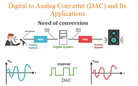
The output from DAC is filtered out to produce Analog signalįig. A Digital to Analog Converter DAC converts a digital input signal into an analog output signal. Functional Software Electrical etc.
The digital signal is represented with a binary code which is a combination of bits 0 and 1. Figure 1 shows a block diagram of a simplified switched-capacitor analog-to-digital converter ADC. Figure 25-1 illustrates a block diagram of the 12-bit ADC.
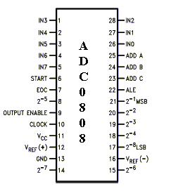
BLOCK DIAGRAM OF A DIGITAL-ANALOG CONVERTER b1 is the most significant bit MSB The MSB is the bit that has the most largest influence on the analog output. ADC Analog-to-Digital Converter Interface with 8086 SOC Start of Conversion EOC End of Conversion ADC 0808 0809 Block Diagram Pin Diagram Successive Approximation ADC. Ad Shop Markertek Products at HuntOffice for a Great Selection of Audio Products.
Ad We Carry All Electronic Parts Components At Surplus Pricing.

Analog To Digital Conversion Adc Analog To Digital Converter Block Diagram Digital
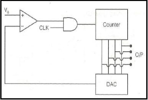
Counter Type Adc Working And Its Advantages And Disadvantages
2

Analog To Digital Conversion Adc Analog To Digital Converter Circuit Diagram Digital
Digital To Analog Converter Dac Architecture And Its Applications
Analog To Digital Converter Block Diagram Types Its Applications

Ltc2644 Dacs Datasheet Cad Models And Features
Analog To Digital Converter Block Diagram Types Its Applications

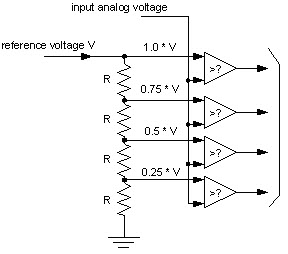
Introduction To Analog To Digital Converters Adc Predictable Designs Analog To Digital Converter Converter Analog
2
Mcp3008 A D Converter Pinout Datasheet Raspberry Pi Setup Video
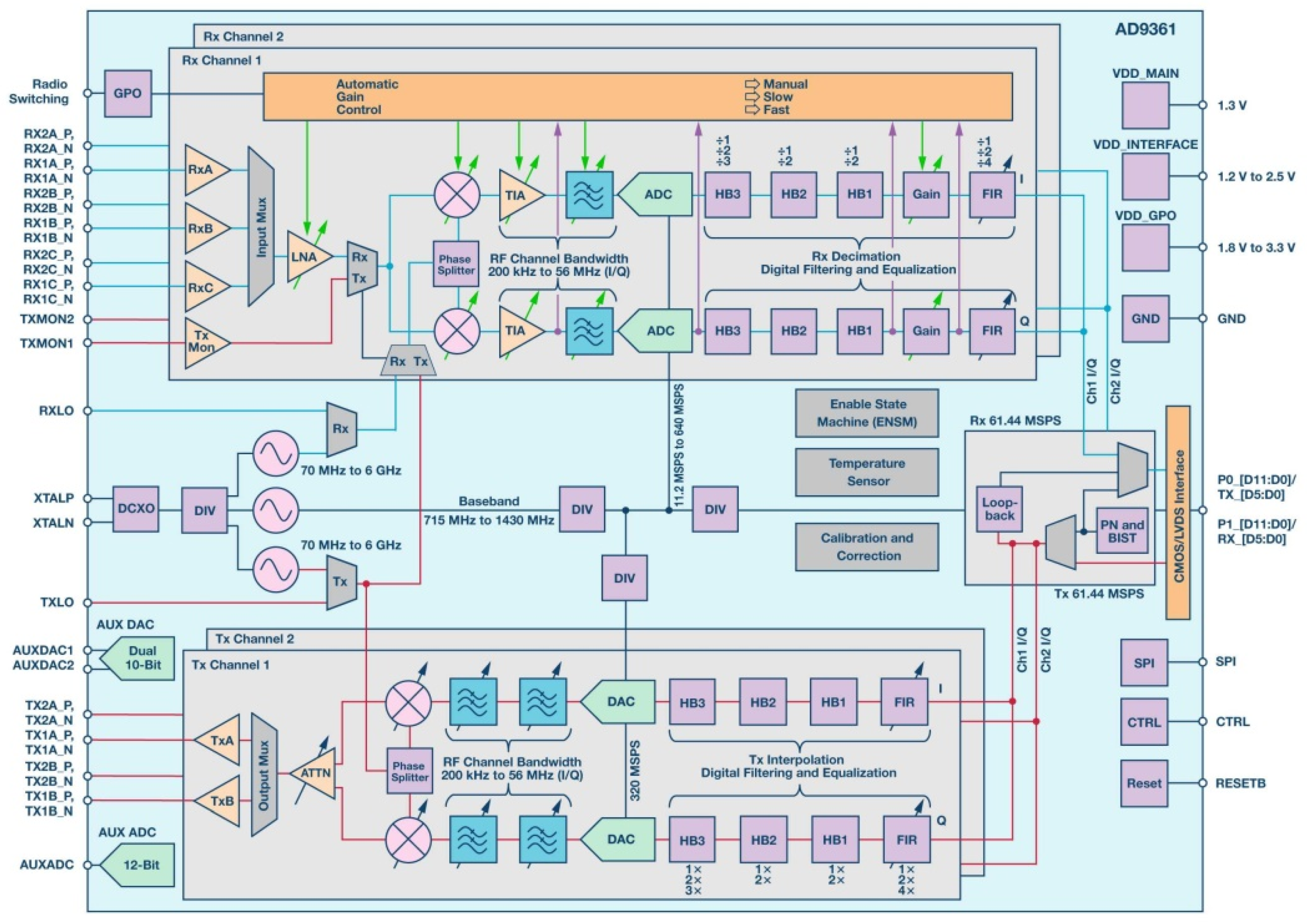
Aerospace Free Full Text Heavy Ion Induced Single Event Effects Characterization On An Rf Agile Transceiver For Flexible Multi Band Radio Systems In Newspace Avionics Html

Added To The Blog Dac Adc Digitaltoanalogconverter Digitaltoanalog Electronic Engineering Analog To Digital Converter Analog
Digital To Analog Converter Dac Architecture And Its Applications

Mcp4728 Dac Datasheet Address Features Video Faq
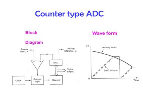
Counter Type Adc Working And Its Advantages And Disadvantages

Hx711 24bit Precision Adc Module Mikroelectron Mikroelectron Is An Online Electronics Store In Amman